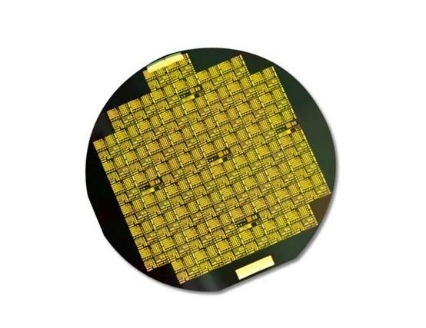
In the rapidly evolving landscape of electronic component technology, High Electron Mobility Transistors (HEMTs) have emerged as a transformative force, especially in high-frequency and high-power applications. These transistors leverage heterostructure materials to create a two-dimensional electron gas (2DEG) channel, enabling superior electron transport properties far beyond those of traditional silicon-based devices.
Core Technical Advantages
HEMTs' most significant advantage lies in their exceptional electron mobility. By utilizing compound semiconductor materials like gallium nitride (GaN) or gallium arsenide (GaAs) in heterostructure designs, HEMTs achieve electron mobilities up to 2,000 cm²/V·s in GaAs-based devices and over 2,500 cm²/V·s in GaN-based variants. In contrast, silicon MOSFETs typically exhibit mobilities below 800 cm²/V·s. This enhanced mobility reduces electron scattering, allowing HEMTs to achieve higher operating frequencies. According to IEEE Microwave Theory and Techniques Society research, GaN-based HEMTs can operate at frequencies exceeding 100 GHz, ten times higher than the upper limit of silicon devices.

In terms of power-handling capabilities, HEMTs outperform traditional transistors significantly. Their high breakdown voltage and low on-resistance enable efficient power conversion. A study by Yole Développement shows that GaN-based HEMTs can handle power densities of up to 10 kW/cm², while silicon devices manage only 1 kW/cm². This results in HEMT-based power amplifiers achieving power-added efficiencies (PAEs) of 70%-80%, compared to 50%-60% for silicon alternatives, greatly reducing energy losses.
Furthermore, HEMTs' heterostructure design allows for precise control over the 2DEG channel. By adjusting material composition and layer thickness, engineers can optimize device performance for specific applications. For example, inserting an aluminum gallium nitride (AlGaN) barrier layer in GaN HEMTs enhances electron confinement, increasing the 2DEG density by up to 5×10¹³ cm⁻² and improving overall device performance.
Disruptive Applications
In the telecommunications sector, HEMTs are revolutionizing 5G and future 6G networks. Their high-frequency capabilities make them ideal for RF power amplifiers. Qualcomm's 5G base station equipment equipped with GaN HEMT amplifiers achieves a 30% increase in output power and a 25% reduction in power consumption compared to previous silicon-based solutions. This not only boosts network coverage but also reduces operational costs for telecom providers.
HEMTs also play a crucial role in electric vehicle (EV) powertrains. Their high-power efficiency optimizes the performance of traction inverters. Tesla's Model Y utilizes GaN HEMT-based inverters, increasing the vehicle's range by 10% through improved energy conversion efficiency. The inverters achieve a peak efficiency of 98.5%, significantly reducing power losses and extending battery life.
In satellite communication systems, HEMTs enable high-data-rate transmission. The European Space Agency's (ESA) latest satellite payloads incorporate GaAs HEMT-based transceivers, achieving data rates of 1 Gbps at frequencies above 30 GHz. These HEMT devices' low noise figures (less than 1 dB) ensure clear signal reception, even in remote orbits.
Challenges
Despite their advantages, widespread adoption of HEMTs faces several hurdles. The primary challenge is the high manufacturing cost of compound semiconductor materials. GaN wafers cost approximately 20 times more than silicon wafers of the same size. Industry efforts aim to reduce GaN wafer costs by 40% by 2026 through techniques like larger wafer sizes (transitioning from 4-inch to 8-inch wafers) and improved epitaxial growth processes.
Reliability under harsh operating conditions also remains a concern. HEMTs can suffer from current collapse and gate leakage issues, especially at high temperatures or high power levels. A field test by a major automotive supplier found that without proper thermal management, GaN HEMTs' failure rate increased by 15% after 1,000 hours of continuous operation at 125°C. Researchers are developing advanced passivation layers and thermal management solutions to address these problems.
Device integration complexity poses another obstacle. Integrating HEMTs with other circuit components requires specialized processes due to material incompatibilities. For instance, combining GaN HEMTs with silicon-based logic circuits demands careful design to avoid thermal stress and electrical mismatches. Developing hybrid integration technologies that balance performance and manufacturability is an ongoing research focus.
This news article details the progress of High Electron Mobility Transistors. If you want articles on other electronic component technologies, or adjustments to the content's depth and focus, feel free to let me know.
-
Wechat

-
Whatsapp
